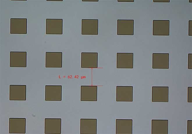
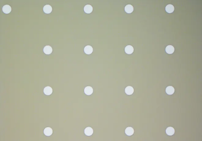
Semicon Global Tech
Photolithography
MEMS Foundry Services
MEMS processing
Photolithography
Lithography
Photolithography Overview
Photolithography is an important step in semiconductor material manufacturing. This process uses exposure and development to define geometric patterns in a photoresist layer, and then transfers the pattern from the photomask to the substrate through etching. Semicon Global Tech provides MEMS foundry services for universities, research institutes and industrial R&D teams, with experience in multiple photolithography technologies.
Applicable Materials
Silicon wafers, glass, sapphire and flexible substrates.
Photolithography Capabilities
Contact Lithography Minimum feature size: 1 μm; overlay accuracy: ±0.5 μm
Stepper Lithography Projection ratio 1:5; minimum feature size: 0.35 μm; overlay accuracy ≤0.15 μm (X, Y); exposure field <22 × 22 mm
Electron-Beam Lithography Minimum feature size: 10 nm; overlay accuracy: 40 nm; exposure range: <100 mm diameter
Case Studies
Photolithographyprocess
Copyright © © Semicon Global Tech Co., Ltd. All Rights Reserved.