Semicon Global Tech
Semiconductor Materials
Silicon Wafers
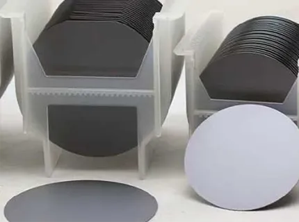
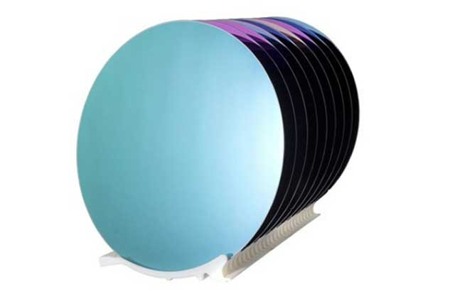
Silicon Wafer Overview
Silicon wafers are core semiconductor substrates supplied in multiple diameters, orientations, resistivity ranges and polishing options for MEMS and IC-related processing.
Silicon Wafer Specifications
Semicon Global Tech supplies semiconductor materials and micro/nano fabrication consumables, including silicon wafers, glass wafers, quartz wafers, PI films, SOI wafers, photomasks and photoresists. Standard specifications and customized processing support are available for MEMS, semiconductor R&D and pilot production projects.
Inch Diameter / mm Polished Side Doping Crystal Orientation Resistivity / Ω·cm Thickness / μm
2inch 50.8±0.5 Double-Side Polished P/N 100 120 200-500
Single-Side Polished
3inch 76 Double-Side Polished P/B 100 NA 525±20
Single-Side Polished
4inch 100±0.2 Double-Side Polished P/N 100 0.001-10 200-2000
100±0.3 Single-Side Polished
100±0.4
6inch 150±0.3 Double-Side Polished P/N 100 110 500-650
Single-Side Polished
8inch 200±0.3 Double-Side Polished P/N 100 0.1-20 625
Single-Side Polished
Learn More
Semiconductor Materials
Glass Wafers
Glass Wafer Overview
Glass wafers provide optical transparency, dimensional stability and bonding compatibility for MEMS packaging, microfluidic chips and laser debonding processes.
Glass Wafer Specifications
Semicon Global Techprovides 4-inch, 6 inch and otherspecificationsBF33glass wafers
Inch Diameter / mm Polished Side Thickness Remarks
4inch 100±0.3 Double-Side Polished 500±10 BF33Glass Wafers
6inch 150±0.3 Double-Side Polished 300,500
Learn More
Semiconductor Materials
Quartz Wafers
Quartz Wafer Overview
Quartz wafers offer optical transmission, thermal stability, chemical resistance and electrical insulation for semiconductor, optical and MEMS applications.
Quartz Wafer Specifications
Semicon Global Tech supplies semiconductor materials and micro/nano fabrication consumables, including silicon wafers, glass wafers, quartz wafers, PI films, SOI wafers, photomasks and photoresists. Standard specifications and customized processing support are available for MEMS, semiconductor R&D and pilot production projects.
Diameter / mm Thickness / mm Remarks
100mm 500um 1mm Please contact us for other sizes
150mm 500um 1mm
100*100mm 160um 500um
100mm 155um 260um
200mm 1mm 2mm
Learn More
Semiconductor Materials
PI Films
PI Film Overview
PI films provide high temperature resistance, chemical stability and flexibility for flexible electronics, sensors, insulation and MEMS device substrates.
PI Film Specifications
Semicon Global Tech supplies semiconductor materials and micro/nano fabrication consumables, including silicon wafers, glass wafers, quartz wafers, PI films, SOI wafers, photomasks and photoresists. Standard specifications and customized processing support are available for MEMS, semiconductor R&D and pilot production projects.
Product Introduction Semicon Global Tech supplies semiconductor materials and micro/nano fabrication consumables, including silicon wafers, glass wafers, quartz wafers, PI films, SOI wafers, photomasks and photoresists. Standard specifications and customized processing support are available for MEMS, semiconductor R&D and pilot production projects.
Thickness Semicon Global Tech supplies semiconductor materials and micro/nano fabrication consumables, including silicon wafers, glass wafers, quartz wafers, PI films, SOI wafers, photomasks and photoresists. Standard specifications and customized processing support are available for MEMS, semiconductor R&D and pilot production projects.
Learn More
Semiconductor Materials
SOI Wafers
SOI Wafers
SOI wafers combine top silicon, buried oxide and handle silicon layers to improve isolation and performance in MEMS and semiconductor devices.
SOI Wafer Specifications
Semicon Global Techcan provide 4-8 inch and otherspecificationsSOIsilicon wafers
Dimensions 4"、5"、6"、8"
process Smart cut:Bonding;SIMOX
types N/P
Top Silicon Layer Thickness 0.22~50μm
Buried Oxide Thickness 0.1~4μm
Handle Layer Thickness 100~500μm
Learn More
Semiconductor Materials
Photomasks
Photomask Overview
Photomasks transfer designed patterns during lithography and can be customized by substrate type, size and pattern precision.
Photomask Types and Process Capabilities
Photomask Types Quartz Substrate
Soda-Lime Glass Substrate
Film Mask
Process Capability 2.5-inch to 9-inch masks can be customized
precision±0.3um
quartz mask precision ±0.1um
Learn More
Semiconductor Materials
Photoresists
Photoresist Overview
Photoresists define micro/nano patterns during exposure and development and support etching, lift-off and high-resolution MEMS fabrication.
Photoresist Specifications
Semicon Global Tech supplies semiconductor materials and micro/nano fabrication consumables, including silicon wafers, glass wafers, quartz wafers, PI films, SOI wafers, photomasks and photoresists. Standard specifications and customized processing support are available for MEMS, semiconductor R&D and pilot production projects.
types Photoresist Model Thickness/um Resolution Applicable process
AZ AZ5214,AZ4620,AZ6130etc. 1-30um 1um can be used for silicon etching
PI LTC9000 4-50um 4um Semicon Global Tech supplies semiconductor materials and micro/nano fabrication consumables, including silicon wafers, glass wafers, quartz wafers, PI films, SOI wafers, photomasks and photoresists. Standard specifications and customized processing support are available for MEMS, semiconductor R&D and pilot production projects.
E-beam Resist HSQ Fox-15/16 100nm 350nm-810nm High-resolution photoresist with etch resistance
Lift-off photoresists LOR/PMGI-SF 50nm-6um Resolution, lift-off
Learn More
Semiconductor Materials
Copyright © © Semicon Global Tech Co., Ltd. All Rights Reserved.