Semicon Global Tech
Etching
MEMS Foundry Services
MEMS processing
Etching
Etching Overview
Etching is the selective removal of unwanted material from the surface of a wafer by chemical or physical methods. It includes material removal by solutions, reactive ions and other mechanical or plasma-based approaches. Etching technologies are mainly divided into dry etching and wet etching. Dry etching uses reactive gases and plasma, while wet etching relies on chemical reactions between etchants and the target material. Semicon Global Tech provides MEMS foundry services and supports multiple etching processes for research and development projects.
Etching Chemicals
Alkaline etchantsKOH, TMAH
Acidic etchantsHF, BOE, HCl, HNO₃, etc.
Etchable Materials
Silicon, silicon oxide, silicon nitride, metals, quartz and other MEMS or semiconductor materials.
Etching Capabilities
Ion Beam Etching (IBE) For metals and other materials that are difficult to etch
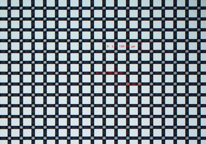
Deep Reactive Ion Etching (DRIE) Etching uniformity <±5%; selectivity >50:1
Reactive Ion Etching (RIE) For etching Si, SiO₂, SiNₓ and related materials
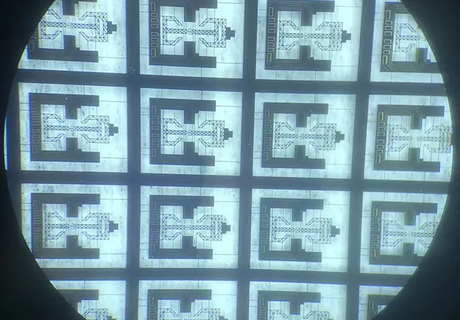
Focused Ion Beam Etching (FIB) Enables micro/nano processing such as etching, deposition and doping on materials and devices
Inductively Coupled Plasma (ICP) Etching For etching GaN, GaAs, InP and other materials
Case Studies
siliconEtching
siliconEtching
Etchingprocess
Etchingprocess
Copyright © © Semicon Global Tech Co., Ltd. All Rights Reserved.