


Engineering teams developing micro-electro-mechanical systems (MEMS)—ranging from automotive pressure sensors and RF acoustic filters to biomedical microfluidics—face a recurring commercial hurdle: transitioning from proof-of-concept CAD models to physical wafer prototypes without exhausting R&D budgets. Traditional Western Tier-1 commercial foundries often impose high non-recurring engineering (NRE) fees, strict minimum order quantities (MOQs) of hundreds of wafers, and queue times reaching 16 weeks or more.
To overcome these roadblocks, university microelectronics labs, fabless MEMS startups, and corporate R&D groups increasingly evaluate MEMS fabrication services from China suppliers. China's semiconductor manufacturing ecosystem has matured into a major hub for specialized micro and nano fabrication. However, evaluating off-shore foundry partners requires a structured methodology to assess technical process limits, cleanroom quality standards, substrate customization flexibility, and design-for-manufacturability (DFM) support.
This guide details a technical framework for evaluating Chinese MEMS foundries, compares core process capabilities, and highlights how an integrated "substrate-plus-foundry" supply chain model accelerates device development cycles.
Selecting a MEMS foundry differs fundamentally from choosing a standard CMOS logic fab. CMOS manufacturing relies on standardized design rules and cell libraries. In contrast, MEMS manufacturing is process-dependent: the device design, structural materials, etch chemistry, and substrate physical properties are tightly interdependent.
When evaluating potential MEMS fabrication services China suppliers, engineering leads should score prospective partners across six core dimensions:
Evaluation Dimension | Key Criteria & Verification Parameters | Why It Matters for MEMS R&D |
|---|---|---|
1. Process Module Match | Capability in DRIE, stepper lithography, thin-film PVD/PECVD, wafer bonding, CMP, and wafer thinning. | Prevents process flow mismatch and costly tool transfer re-engineering. |
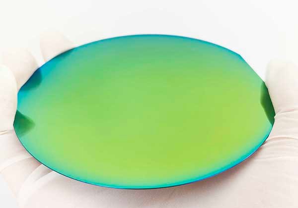
2. Substrate & Material Portfolio | In-house availability of prime silicon, custom SOI, high-purity quartz, and Pyrex glass wafers. | Eliminates multi-vendor interface delay and ensures mechanical/thermal compatibility. |
3. Prototyping Batch Flexibility | Willingness to run small R&D pilot runs (5 to 50 wafers) with short turnaround times (4 to 8 weeks). | Preserves R&D grant budgets and enables rapid iterative design validation. |
4. Cleanroom & Quality Standards | ISO 9001 certified operations, ISO Class 5 (Class 100) lithography bays, in-line SPC, and automated optical inspection. | Directly determines wafer yield stability, defect density, and lot-to-lot repeatability. |
5. DFM Co-Engineering Support | Dedicated process engineering review of mask layouts, design rules, stress management, and etch selectivity. | Identifies lithography shadowing, wafer bow, and stiction risks before mask glass fabrication. |
6. IP Protection & Traceability | Documented customer non-disclosure agreements (NDAs), encrypted mask file transfers, and lot-level tracking. | Protects proprietary sensor topologies and trade secrets during overseas pilot production. |
A capable MEMS foundry must demonstrate deep technical mastery across several foundational process modules. When reviewing a foundry's process capability matrix, look beyond generic equipment lists and verify specific operational boundaries.
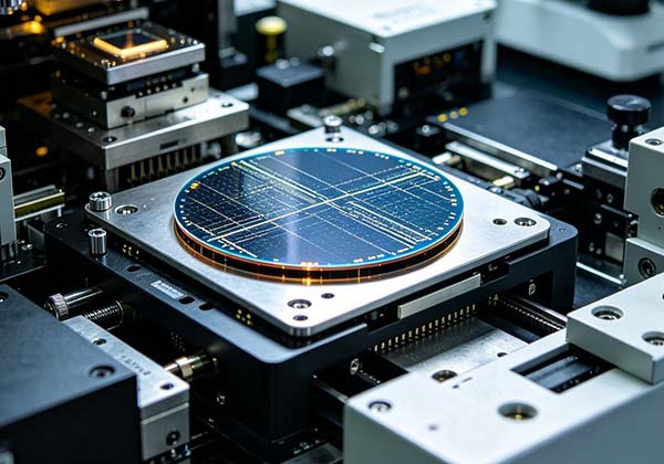
Lithography defines the lateral feature resolution and alignment accuracy across substrate layers. MEMS devices often require patterning over deep topography or inside etched cavities, which demands specialized resist coating and exposure capabilities.
Pro Tip: When designing high-aspect-ratio microstructures, confirm whether your foundry supports thick photoresists (such as SU-8 or polyimide up to 50µm thickness) alongside double-sided mask alignment for back-side cavity etching.
High-precision foundries offer advanced lithography patterning services supporting contact aligners, reduction steppers, and direct-write electron-beam lithography (EBL) for sub-micron features down to 0.5µm.
Deep Reactive-Ion Etching using the Bosch time-multiplexed process is the workhorse technology for bulk micromachining. It creates vertical, high-aspect-ratio silicon structures such as comb-drive actuators, flexures, and sensor beams.
When evaluating DRIE capabilities, verify:
Aspect Ratio Limit: Aspect ratios exceeding 20:1 or 30:1 for narrow silicon trenches.
Sidewall Profile Control: Vertical sidewall angles controlled within 90° ± 0.5° with minimal scalloping roughness.
Etch Uniformity: Total Thickness Variation (TTV) and etch rate uniformity within ±3% across 4-inch, 6-inch, or 8-inch wafers.
Structural, sacrificial, insulating, and conductive thin films form the functional layers of MEMS sensors. Foundries must provide diverse deposition techniques to balance film stress, stoichiometry, and step coverage:
Physical Vapor Deposition (PVD): Sputtering and e-beam evaporation for noble metals (Au, Pt, Al, Ti/Pt, Cr/Au) used in electrical contacts, mirror coatings, and interconnects.
Chemical Vapor Deposition (CVD/PECVD/LPCVD): Low-stress silicon nitride (SiN), silicon dioxide (SiO₂), and polysilicon layers for structural membranes and electrical isolation.
Atomic Layer Deposition (ALD): Conformal atomic-scale oxide and nitride coatings for microfluidic channel passivation and bio-compatibility.
Partners offering specialized thin-film deposition capabilities allow engineers to adjust film stress profiles precisely, preventing wafer bow during thermal cycling.
Wafer-level bonding integrates multi-substrate stacks and provides vacuum-sealed cavity packaging for resonant sensors and gyroscopes:
Silicon Fusion Bonding: Direct high-temperature bonding of silicon-to-silicon or silicon-to-oxide for SOI substrate fabrication and pressure sensor diaphragms.
Anodic Bonding: Electrostatic bonding of silicon to borosilicate glass (Pyrex 7740) at moderate temperatures (300°C–400°C), widely used in microfluidics and capacitive accelerometers.
Eutectic & Glass Frit Bonding: Low-temperature metallic bonding (e.g., Au-Si, Al-Ge) for hermetic wafer-level capping.
After front-end wafer fabrication, wafers undergo backgrinding, Chemical Mechanical Planarization (CMP), through-wafer micro-drilling, and precision stealth dicing. Wafer thinning down to 100µm or less is essential for compact sensor packaging and flexible electronics.
A major challenge when outsourcing MEMS prototyping is supply chain fragmentation. Traditionally, an R&D team must buy specialized engineered wafers from a materials distributor, ship them to a third-party cleanroom for lithography and etching, and send processed wafers to an OSAT vendor for dicing and packaging.
This multi-vendor model introduces significant operational risks:
Material Mismatch: Non-standard wafer thickness or surface roughness causing handling errors on foundry robotic end-effectors.
Finger-Pointing on Yield: Substrate vendors blaming processing stress for wafer cracking, while the foundry blames raw wafer defect density.
Accumulated Lead Times: Multiple transit legs and vendor qualification queues stretching project timelines past grant or funding deadlines.
Traditional Fragmented Model:
Substrate Vendor → Transport → Fab Cleanroom → Transport → Packaging House
(High lead time, split quality accountability, multi-margin cost)
Integrated Supply Model:
Substrate Manufacturing + Micro/Nano Fabrication + DFM Review (Under One Roof)
(Lower overhead, single point of contact, guaranteed material-process compatibility)
Leading Chinese suppliers solve this problem by providing an integrated model that combines raw substrate manufacturing with full-process micro/nano foundry execution.
Having immediate, in-house access to custom substrates enables process engineers to tune substrate specifications directly to the device architecture:
Substrate Material Type | Key Material Characteristics | Primary MEMS Applications |
|---|---|---|
Silicon-on-Insulator (SOI) Wafers | Precise single-crystal device layer (0.5µm–100µm), buried oxide (SiO₂) etch stop layer, low stress. | High-precision pressure sensors, optical MEMS mirrors, silicon photonics, micro-gyroscopes. |
Prime Silicon Wafers | High-purity CZ/FZ single-crystal silicon, controlled resistivity, custom orientation (<100>, <111>). | Piezoresistive sensors, thermal actuators, bulk-micromachined structures, CMOS-MEMS integration. |
High-Purity Quartz Wafers | Exceptional thermal stability, near-zero thermal expansion coefficient, high optical transparency, low RF loss. | High-Q RF MEMS resonators, optical windows, SAW filters, high-temperature sensors. |
Pyrex / Glass Substrates | Matches silicon's coefficient of thermal expansion (CTE), excellent optical transmission, anodic bondable. | Microfluidic lab-on-chip devices, bio-MEMS, optical windows, capacitive sensor bases. |
By utilizing specialized custom SOI (Silicon-on-Insulator) wafers with custom device layer thicknesses and tight TTV tolerances, sensor designers can eliminate timed silicon etch steps, achieving near-perfect diaphragm thickness control across the entire wafer batch.
Similarly, sourcing prime single-crystal silicon wafers in 2-inch to 8-inch diameters, or utilizing high-purity quartz substrates and MEMS glass substrates and microfluidics, ensures optimal optical, mechanical, and dielectric performance for specialized applications.
Located in the semiconductor manufacturing cluster of Changzhou, Jiangsu, China, Semicon Global Tech (SGT) represents this modern, integrated approach to semiconductor materials and foundry services.
With over a decade of integrated R&D and manufacturing experience holding more than 28 certified qualifications and honors, Semicon Global Tech provides comprehensive one-stop MEMS foundry services tailored for global research institutes, universities, and fabless MEMS enterprises.
Semicon Global Tech (SGT) Integrated Capability Stack:
Lithography • DRIE Etching • Thin-Film Deposition • Bonding
Full-Process MEMS Foundry Engineered Substrate Manufacturing Silicon Wafers • Custom SOI • Quartz • Pyrex Glass DFM Co-Engineering & Quality Assurance Mask Review • ISO 9001 Controls • In-Line Metrology
Integrated Substrate & Fab Supply: SGT manufactures silicon, SOI, quartz, and glass wafers in-house, eliminating substrate sourcing delays and guaranteeing material purity for downstream processing.
R&D & Prototyping Flexibility: Unlike Tier-1 foundries that demand high-volume commitments, SGT accommodates small-batch R&D runs (5 to 50 wafers) as well as pilot-scale volume expansion.
Full Process Coverage: SGT executes complete micro/nano fabrication workflows—including contact/stepper lithography, high-aspect-ratio DRIE, PECVD/PVD film deposition, anodic and fusion bonding, wafer thinning, and stealth dicing under one roof.
Dedicated DFM Engineering Support: SGT's technical team collaborates directly with customer design engineers to review GDSII/OASIS layout files, optimize process tolerances, and select ideal substrate dopants before mask fabrication begins.
Standard prototype wafer fabrication cycles typically range between 4 and 8 weeks, depending on mask layer count and process complexity. Foundries with in-house substrate manufacturing like Semicon Global Tech can shorten lead times by eliminating raw material procurement delays.
Reputable Chinese MEMS foundries operate under strict non-disclosure agreements (NDAs), encrypted file transfer protocols for GDSII mask data, and isolated job-tracking systems in ISO-certified cleanrooms.
Cavity SOI wafers contain pre-etched, vacuum-sealed cavities beneath a single-crystal silicon device layer. This allows sensor developers to fabricate ultra-thin, uniform diaphragms for pressure sensors and microphones using a single planar etch step, eliminating complex back-side bulk micromachining.
Yes. Agile foundries can process non-standard wafer diameters (such as 2-inch, 3-inch, or 4-inch substrate fragments) alongside standard 6-inch and 8-inch lines, which is ideal for costly specialized materials like quartz or custom-doped SOI.
Selecting the right fabrication partner is the single most critical decision in bringing a novel MEMS device from CAD design to market reality. By choosing an integrated supplier that combines custom substrate manufacturing with comprehensive micro/nano fabrication capabilities, engineering teams drastically reduce development costs, eliminate supply chain friction, and accelerate prototype iteration cycles.
Whether you require custom-designed SOI wafers, high-aspect-ratio DRIE etching, low-stress thin-film deposition, or a full-process turnkey foundry run, Semicon Global Tech offers the expertise, certified cleanroom infrastructure, and batch flexibility your project demands.
contact Semicon Global Tech for DFM review today to submit your GDSII layout files, request a substrate quotation, or discuss your customized MEMS fabrication roadmap with a senior process engineer.